Machinery / Semiconductors and Automation
Die Bonders
Iwatani offers advanced one-stop solutions that encompass all processes encountered in the semiconductor manufacturing sector.
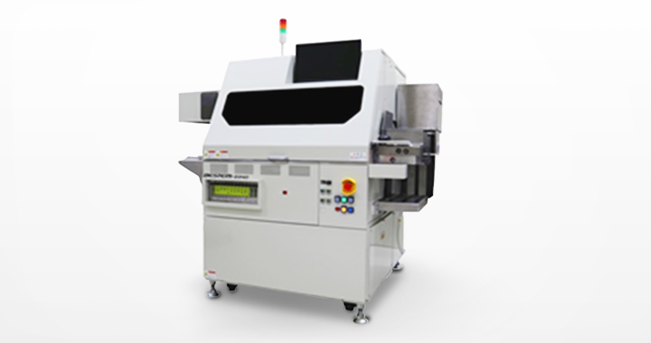
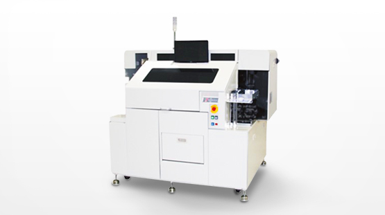
Soft Solder Die Bonder (8-Inch)
Die Bonder for Solder Bonding Processes for Power Devices Requiring High Quality Bonding
Features
- Incorporates high performance reduction feeder for solder fusing bonding.
- Incorporates solder spanker (forming) function for high bonding quality.
- Supports large frames up to 100 mm wide.
- Provides flexible support for wafer mapping and traceability.
- Supports wafer sizes up to 8-inch diameter
Specifications
| Bonding Method | Wire solder feed bonding |
|---|---|
| Bonding Speed UPH | 6,000 (with SOP8 continuous matrix frame and chip size equivalent to 3-mm square) |
| Bonding Accuracy (Using CU Island, Spanker, and Pyramidal Collet) | XY: ±38 µm (3σ) |
| Θ: ±1° (3σ) | |
| Chip Size | 1 to 11-mm square *Optional: 15-mm square |
| Lead Frame Size |
|
| Magazine Size |
|
| Wafer Size | Max. 8-inch diameter |
| System Size |
|
| Weight | Approx. 1,600 kg |
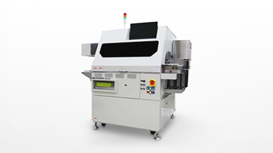
Soft Solder Die Bonder (12-Inch)
Die Bonder for Solder Bonding Processes for Power Devices Requiring High Quality Bonding
Features
- Incorporates high performance reduction feeder for solder fusing bonding.
- Incorporates solder spanker (forming) function for high bonding quality.
- Supports large frames up to 100 mm wide.
- Provides flexible support for wafer mapping and traceability.
- Supports wafer sizes up to 12-inch diameter.
Specifications
| Bonding Method | Wire solder feed bonding |
|---|---|
| Bonding Speed UPH | 6,000 (with SOP8 continuous matrix frame and chip size equivalent to 3-mm square) |
| Bonding Accuracy (Using CU Island, Spanker, and Pyramidal Collet) | XY: ±38 µm (3σ) |
| Θ: ±1° (3σ) | |
| Chip Size | 1 to 11-mm square *Optional: 15-mm square |
| Lead Frame Size |
|
| Magazine Size |
|
| Wafer Size | Max. 12-inch diameter |
| System Size |
|
| Weight | Approx. 2,000 kg |
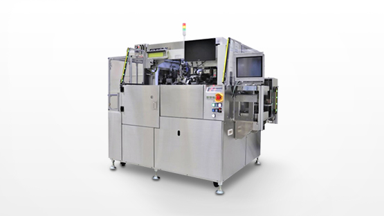
Epoxy Die Bonder
High-Speed, High-Precision Die Bonder Supporting 12-Inch Wafers for IC/Lsi Applications
Features twin dispenser to give high UPH. Uses a unique pick-up system to enable picking up down to a minimum thickness of 15 µm.
Features
- High throughput, small footprint, with quick product switching time, reducing TCO.
- Easily adjustable and includes a reworking function for outstanding ease of operation.
- Minimizes distances between mount positions and preforms, prevents variations over time, and reduces wasteful movements.
- Incorporates newly-developed twin dispensing system to support wide-ranging pastes
- Needle-free pick-up system (optional) enables damage-free pickup
Specifications
| Bonding Method | Epoxy bonding/thermocompression bonding (option) |
|---|---|
| Bonding Speed | 0.18 s/cycle |
| Bonding Accuracy | XY: ±25 µm, 3σ |
| θ: 1°, 3σ (1.0-mm square or over) | |
| θ: 3°, 3σ (under 1.0-mm square) | |
| Chip Size | 0.3 to 8.0-mm square t = 0.075 to 0.5 mm Optional: 0.15 to 2.0-mm square (identification lens change) |
| Lead Frame Size |
|
| Magazine Size |
|
| Wafer Size | Max. 12-inch diameter |
| Utilities |
|
| System Size |
|
| Weight | Approx. 1,600 kg |
| Optional Features |
|
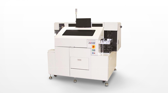
Die Sorter
Only Good Quality Dies Are Picked Up from Diced Wafers, Then Arranged/Stored on a Tray Extensive Proven Support from Mems to IGBT and CMOS Sensors
Features
- High-precision sorting XY: ±38 µm (3σ)
- Supports 6, 8, 12-inch wafers using the change kit
- Supports thin dies using (optional) unique needle-free pickup technology
Specifications
| Wafer Size | 6, 8, 12-inch square |
|---|---|
| Chip Size | 1.5 to 25-mm square |
| Conveyable Tray Size | 2, 3, 4-inch square |
| Layout Accuracy | XY: ±38 µm (3σ) |
| Unit Size |
|
| Weight | Approx. 1,600 kg |
Bonding Tester
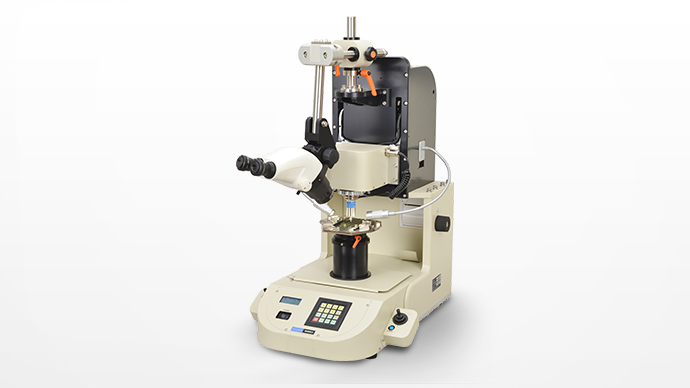
From Next Generation Mounting R&D to Quality Control Semiconductor Post-Processing Bond Strength Evaluation Using a Single Unit
Features load detection accuracy and fine adjustment accuracy for measuring gold wire pull (tensile) strength and ball shear strength. Switches sensors to maintain accuracy in low-load regions, even in high-load region measurements, including measurements of die shear strength and solder bond strength.
Features
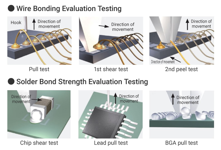
- Capable of evaluating Au, Al, Cu, and ball, wedge, ribbon, and die bonding.
- The measuring direction and speed is kept constant using three-axis drive control to ensure that consistent results can be obtained by anyone easily.
- Numerical evaluations based on test methods that meet Japanese and international requirements and standards
- ● JIS Z 3198-6/7
- ● MIL-STD-883
- ● JEITA ED 7403/7407
- ● IEC 749
- ● JEITA ED 4703
- ● SEMI G73-0997
Measurement Examples
Specifications
| Measured Load Range | Pull test Push test Peel test |
Max. 20 kg |
|---|---|---|
| Shear test | Max. 100 kg | |
| Measurement Accuracy | ±0.2%FS | |
| Measurement Speed Range | Pull test Push test Peel test |
0.001 to 5 mm/s |
| Shear test | 0.001 to 10 mm/s | |
| Drive Range | X axis | ±50 mm |
| Y axis | ±50 mm | |
| Z axis | Max. 70 mm | |
| Observation Direction | Vertically | 45° |
| Horizontally | ±90° control |
Please inquire for more information on die bonders.
Electronics Equipment Department
Tokyo
81-3-5405-5781
Osaka
81-6-7637-3072