Machinery / Semiconductors and Automation
Trim and Forming Systems, Dies
Iwatani offers advanced one-stop solutions that encompass all processes encountered in the semiconductor manufacturing sector.
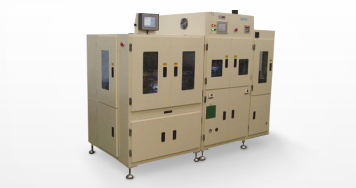
Trim and Forming Systems (TF Systems)
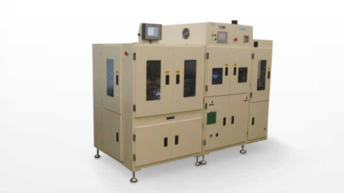
Lead Processing Systems, With High Shipment Track Record Can Be Combined With Ld/Uld, Printing, and Inspection to Combine Individual Processes, Offering Labor and Manpower Savings.
The design can be customized to allow movement of items between systems. Numerous combined systems have been shipped to date in conjunction with pre- and post-processing systems.
Features
Easy customization allowing flexible configuration, with track record of high shipments in conjunction with pre- and post-processing systems
Main combined systems
- Lead frame loader
- Unloader units, including magazine storage
- Printing units, including laser processing units
- Inspection systems based on image recognition cameras
Customizable design, offering wide-ranging layouts to suit requirements
Main Configurations
- Loader (e.g., stacks, slits, trays, sticks, reels)
- Unloader (e.g., stacks, slits, trays, sticks, reels)
- Laser markings
- Image recognition inspections
- Testing (e.g., OS, characteristics)
Customizable design, offering wide-ranging layouts to suit requirements
Main Specifications
Extensive range available, with processing capacity up to standard 6 t to meet customer requirements
TF Dies
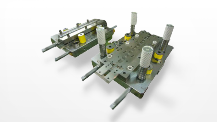
Offering Die Configurations Incorporating Special Cam or Roller Bending to Minimize Package Damage
- Removal technology (minimizing scrap rising and blockage)
Die, punch, and product receptacle profiles are configurable to prevent damage to both products and dies. Iwatani offers optimal profile solutions. - Bending technologies
Traces of contact with the product are minimized to improve product appearance and plating adhesion to die components. Optimal bending solutions, such as cam and roller bending, are offered to suit product profiles. - Die life improvements
Changes to cutting tool materials and special coatings help extend the die life.
Main Applications
Trim and form dies are used at the final stage of semiconductor production to cut out individual packages and form leads.
- Resin cutting
Punching (resin) burrs on parts enclosed by the package exterior, tie bars, or leads - Tie bar cutting
Punching tie bars - Lead cutting
Cutting lead ends and individual packages - Lead forming
Bending lead ends to their final shape
Typical Applications
- SOP products
- DIP products
- SOT products
- SON products
Laser Processing System (Marking, Deburring, Resin Removal)
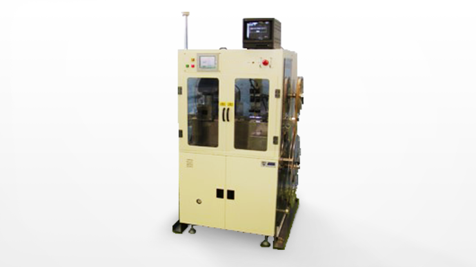
Lower Semiconductor Defect Rates Achieved Using Laser Irradiation
This system is designed to stamp semiconductor component products. It allows printing on components for each frame, individual components, and two-dimensional code printing. Laser irradiation can also be used to deburr resin components and remove resin. Resin removal is traditionally a process performed using dies. However, in addition to reducing semiconductor defect rates, a laser system helps eliminate die maintenance requirements (for example, replacement work associated with die and punch wear).
Main Applications
Used in processes to stamp product names, manufacturer names, and lot numbers on package surfaces, primarily after cutting out individual packages and forming leads
Typical System Configuration
- Frame supply unit
- Orientation/product confirmation unit (option)
- Laser marking unit
- Visual inspection unit (option)
- Brush unit (option)
- Frame storage unit
Please inquire for more information on trim and forming systems and dies.
Electronic Equipment Department
Tokyo
81-3-5405-5781
Osaka
81-6-7637-3072