Machinery / Semiconductors and Automation
Semiconductor and Electronic Component Inspection Systems
Iwatani offers advanced one-stop solutions that encompass all processes encountered in the semiconductor manufacturing sector.
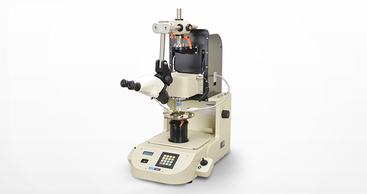
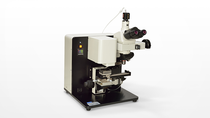
Bonding Tester
From Next Generation Mounting R&D to Quality Control Semiconductor Post-processing Bond Strength Evaluation Using a Single Unit
Features load detection accuracy and fine adjustment accuracy for measuring gold wire pull (tensile) strength and ball shear strength. Switches sensors to maintain accuracy in low-load regions, even in high-load region measurements, including measurements of die shear strength and solder bond strength.
Features
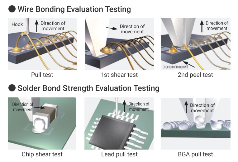
- Capable of evaluating Au, Al, Cu, and ball, wedge, ribbon, and die bonding.
- The measuring direction and speed is kept constant using three-axis drive control to ensure that consistent results can be obtained by anyone easily.
- Numerical evaluations based on test methods that meet Japanese and international requirements and standards
- ● JIS Z 3198-6/7
- ● MIL-STD-883
- ● JEITA ED 7403/7407
- ● IEC 749
- ● JEITA ED 4703
- ● SEMI G73-0997
Measurement Examples
Specifications
| Measured Load Range | Pull test Push Test Peel test |
Max. 20 kg |
|---|---|---|
| Shear test | Max. 100 kg | |
| Measurement Accuracy | ±0.2%FS | |
| Measurement Speed Range | Pull test Push test Peel test |
0.001 to 5 mm/s |
| Shear test | 0.001 to 10 mm/s | |
| Drive Range | X axis | ±50 mm |
| Y axis | ± 50 mm | |
| Z axis | Max. 70 mm | |
| Observation Direction | Vertically | 45° |
| Horizontally | ±90° control |
Solder Checker
Measures Solder Wettability Against Time on Electronic Components
Despite the rapid progress made in reducing the size of electronic components in high-precision mounting, this system is capable of measuring even the latest microscopic electronic components. Solder wettability testing (wetting balance testing) is stipulated in Japanese and international standards as a test method for quantitatively evaluating solder wettability. This single device can be used to perform a wide range of tests, including the most fundamental solder bath balancing method, small solder sphere balancing method for evaluating surface-mounted components, and rapid heating method and profile heating method for evaluating surface-mounted components using solder paste.
Features
- Allows high-precision evaluation of 0603 and 0402 microscopic chip components.
- Includes chucks to suit various components, allowing evaluation of a wide range of configurations.
- The temperature profile method allows fine heating behavior to be set using temperature settings for 16 zones.
- Can also be used for analyzing the behavior of halogen-free low-temperature solder paste and also N2 gas purging.
- The wetness state can be observed using a high-speed (430 FPS) camera or alignment camera.
- The X-Y stage is motor driven to allow precise positioning (with LED light).
- The lineup includes a standard type, high-sensitivity type, and low-cost type to suit individual applications.
- Allows evaluation with any kind of solutions
- Allows evaluation of powders in solution
Specifications
| Measuring Range | ±10 mN, 50 mN | |
|---|---|---|
| Temperature Setting Range | Room temperature to 450°C | |
| Temperature Accuracy | ±2°C (for 245°C setting) | |
| Solder Pot | 60 mm diameter, 30 mm deep (60 mm deep pot can also be used) | |
| Immersion Time | 1 to 999 s, 1 to 999 mins | |
| Immersion Depth | 0.01 to 1 mm | 0.01 mm steps |
| 1 to 20 mm | 0.1 mm steps | |
| Immersion Speed | 0.1 to 1 mm/s | 0.1 mm/s steps |
| 1 to 5 mm/s | 0.5 mm/s steps | |
| 5 to 30 mm/s | 5 mm/s steps | |
| Stress Precision | ±0.1%FS (0.01 mN for 10 mN setting, 0.05 mN for 50 mN setting) | |
| Time Axis Response | 0.14 s (zero to full scale) | |
| Stage Movement Distance | X-axis: ±5 mm, Y-axis: ±5 mm | |
| Sample Weight | 10 g | |
| Power Supply | 100 V to 220 V AC ±10% 50/60 Hz | |
| Power Consumption | 600 W | |
| Weight | 45 kg | |
| Dimensions |
|
|
| Options | Small solder sphere balancing method kit, rapid heating method unit, profile heating method unit, alignment camera unit, high-speed wetness image analysis system | |
| Dynamic wettability testing kit, acrylic wind shield, N2 chamber, active micro-vibration control system | ||
Scratch Tester
Quantitative Measurement of Adhesion Strength of Submicron Thin Films
This is a testing machine capable of evaluating the adhesion strength of submicron thickness ultrathin films using the micro-scratch method (conforming to JIS R 3255 and JIS K 7376), a development of the scratch method used to evaluate the adhesion strength between a substrate and a thin film deposited on its surface through the ability to detect peeling of even thinner films. In addition to the micro-scratch method specifically suitable for thin film damage detection, the machine also features a proprietary (Pat. No. 5070146) high-sensitivity damage detection mechanism for evaluating the adhesion strength of ultrathin films.
Features
- Capable of evaluating adhesion strength of submicron thickness ultrathin films.
*Measurements achieved in practice down to 10 nm film thickness - Capable of evaluation during sample heating
- Capable of measuring curved samples such as lenses
- Capable of evaluating coefficient of friction for 100 µm × 100 µm areas using time-series friction histogram (TSFH) analysis
Applications
- DLC
- Optical thin films
- Metal thin films
- PET thin films
- Function thin films (AR, RF)
- Electrode films, etc.
Specifications
| Load Detection Mechanism | Loading range | 1 to 1,500 mN |
|---|---|---|
| Load resolution | 0.3 mN | |
| Allowable overloading | 300%FS | |
| Horizontal Signal Output | Detection signal | Speed signal |
| Frequency range | 20 Hz to 10 kHz | |
| Excitation frequency | 45 Hz | |
| Excitation amplitude | 0, 5, 10, 20, 40, 50, 80, 100 µm | |
| Perpendicular Signal Output | Detection signal | Acceleration signal *Patented technology |
| Frequency range | 20 Hz to 10 kHz | |
| Probe | Material and shape | Diamond (R5, 10, 15, 25, 50, 100 µm) |
| Sapphire (R250, 500 µm) | ||
| 3/32 inch diameter ball can be attached | ||
| Z-Axis Drive Mechanism | Drive system | Stepping motor drive |
| Loading Direction | Drive range | 20 mm (manual +30 mm coarse movement range available) |
| Drive resolution | 0.5 µm | |
| Drive speed (for measurement) | 0.1 to 10 µm/s | |
| Drive speed (for setup) | 1 mm/s | |
| X-Axis Drive Mechanism | Drive system | Stepping motor drive |
| Scratch Direction | Drive range | 20 mm |
| Drive resolution | 0.5 µm | |
| Drive speed (for measurement) | 0 to 20 µm/s | |
| Drive speed (for setup) | 1 mm/s | |
| Sample Stage Xy Axis Drive Mechanism | Drive system | Manual drive using micrometer |
| Drive range | ±6.5 mm | |
| Data Output Method | USB | |
| Dimensions and Weight |
|
|
| Power Supply | 100 V to 240 V AC |
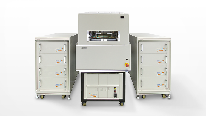
Accelerated Life Testers (HAST Testers)
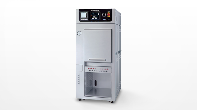
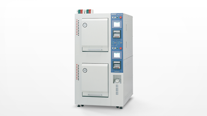
For Accelerated Life Evaluation of Semiconductors, Electronic Components, and Materials
In the semiconductor and electronic components industry, progress in miniaturization and higher density is advancing rapidly, making improved reliability, together with assessment thereof key issues. Systems offered by Iwatani meet such needs with wide dimensions using twin-chamber configurations.
Features
- Sliding tray system for ease of operation.
- Twin-chamber system with independent test chamber and vapor generation chamber, offering a wide effective area and enabling wide-ranging operating humidity
- Supports two control methods (unsaturated control, saturated control)
- Supports three exhaust modes (constant-humidity slow cooling mode, moisturizing cooling mode, rapid exhaust mode)
- Voltage application connectors located inside the door, for easy connection
- Electro-polished chamber interior prevents dirt adhesion and ensures easy cleaning
Microfocus X-Ray Inspection System
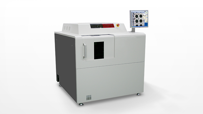
Inspects Internal Defects With High Precision Using Sharp Imagery
This system is capable of testing and analyzing non-destructively and is compatible with the reduced size, increased density, and BGA/CSP bonding techniques increasingly used in the semiconductor industry. It combines a proprietary microfocus X-ray generator with a high performance X-ray detector to produce high-resolution, high-magnification X-ray images. All processes from scanning to imaging are controlled via a PC for ease of operations, and systems can be built to order to suit customers’ particular samples.
Fully-Automated Electrostatic Breakdown System
Testing System Supporting Hbm/MM Using Capacitor Discharge Effective for Esd Testing of Multi-Pin Semiconductors With More Than 1,000 Pins
Allows testing in compliance with international standards (JEDEC, ESDA, AEC, and JEITA). This system’s unique short-circuit discharge circuits were made possible using proprietary machine design. Short-circuiting minimizes the effects of inductance and capacitance on data. And use of a single circuit guarantees consistency among data for each device pin tested.
Compact ESD Tester
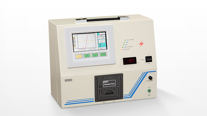
Testing Device Supporting Hbm/MM Using Capacitor Discharge Effective for Esd Testing of Semiconductors With Small Number of Pins
Easy-to-operate portable electrostatic breakdown tester. It also features a leak measurement function, enabling breakdown due to ESD to be determined using this device on its own.
Probing Handler
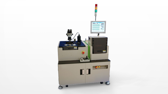
Probing Inspection of Diced Wlcsps and Package Substrates
A unique concept enabling diced WLCSPs and package substrates (e.g., BGA, QFN) to be inspected using probing in a handler unit. The proprietary XY positioning correction function and profiling function enables probing supporting multiple simultaneous measurement by correcting positioning offsets after dicing caused by distortion/flexing due to film tension or dicer blades.
Features
- Supports diced WLCSPs and package substrates (e.g., BGA, QFN)
- Corrects positioning after dicing, allowing probing supporting multiple simultaneous measurement
- Also supports inspection by re-affixing chips to film frame
- Allows probing of multiple points within a single chip
- Uses ring clamp system to eliminate effects of film sagging
- Supports small chips below 1 mm size using small-diameter VAC holes
- Features chuck surface sandblasting treatment and air-blower mechanism to improve film removal
- Low noise: -80 dB or lower above chuck (Reference value: Loop ANT measurement data for 30 kHz to 30 MHz)
- Supports even small chips below 0.5 mm in size using ultra-small-diameter VAC holes (option)
- Supports high temperature (50°C to 150°C) testing and high-precision (25°C ±0.3°C) temperature control function (option)
- Non-magnetic specifications compatible with magnetic devices.
*Reference data (standard model): 0.04 mT above chuck, 0.2 mT above feed route
Please inquire for more information on semiconductor and electronic component inspection systems.
Electronic Equipment Department
Tokyo
81-3-5405-5781
Osaka
81-6-7637-3072